I had been planning to use a DIN 6 pigtail to connect the bread boarded adapter to my coco but then I noticed I had a DIN 6 to DIN 6 cable and the DIN 6 sockets I planned to use in the final project so I decided the easy thing to do would be to create a breakout PCB for the socket. This would also give me the benefit of learning KiCad on a much simpler project than the final Arduino shield I’d like to design.
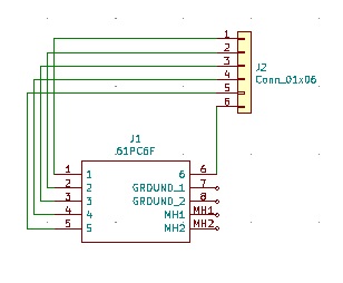
I downloaded KiCad and installed it and then I fought for a while with getting Mouser’s symbol library loader configured. Finally the library loader popped up a very helpful help page in my browser and after following the pre-configuration steps I could see the symbols for the DIN 6 socket in the symbol library. When wiring up the connections between the DIN 6 and the 6 pin header I discovered that if a wire lays directly on top of another wire KiCad will automatically join them as the same wire in the schematic. Finally I ended up with a final schematic like this.
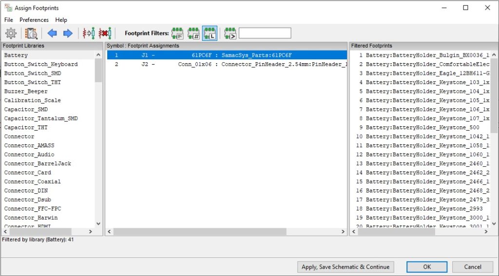
The next step was to produce a PCB layout from the schematic. I clicked the button to populate a layout from the schematic and was instantly faced with errors. The symbols on the schematic were not associated with layout footprints and could not be auto-associated. I opened the association dialog and it took a fair while to figure out what needed to be done. The left column contains the libraries so select the library your part is in. This filters what you see in the right most column. Next click on the component you want to associate and then double-click the appropriate part in the right most column. You know you you have done it correctly when you see the name of the footprint next to the name of the schematic symbol in the middle column. When you assign all of your footprints you can click ok.
The next issue I ran into when I tried to generate the layout was the lack of a netlist. This was remedied by clicking the “net” button and clicking “Generate Netlist” in the Pcbnew tab. When this was done I was able to press the button to run pcbnew to create a layout. You will see your component footprints attached by grey lines that represent the wires from the schematic.
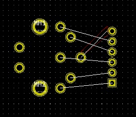
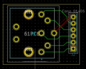
The grey lines represent the connections you made in the schematic but they are not yet traces. The need to be routed. I spent some time trying to get autorouting to work but it seems you need external tools for that which I was unable to get working. I left that as a task for later and instead used the manual routing tool. You click on the pad you want to start with and then drag to create trace. If you need to route around something, like when routing between the middle pad above and its associated pin, you can use several clicks on your way to the connected pad to lock in corner locations for your trace route. Also notice that there are some of the network lines that cross over each other, those had to be handled by putting the trace that does the crossing on a different layer from the traces that don’t cross. It was also necessary to add PCB edge lines using the line tool on the edge cuts layer. In the end I had a layout.
Next I generated the gerber files by using the plot function. I chose the layers that were useful in my project. These were the front and back copper layers, front and back silkscreens, front and back solder mask and the edge cuts layer. When the right layers were selected I clicked the plot function and got a set of gerber files. I also generated the drill file with the drill file tool in the fabrication outputs submenu of file. At this point I had what I needed for Oshpark which is the board house I chose to manufacture this PCB.
Oshpark has low order minimums, 3 boards, and reasonable prices. The package format I chose to submit my design as was a zip of gerbers which I made by taking all of my gerber files, generated during the plot function, and the drill file and putting them into a single zip file. On the site I uploaded this this zip file on the main page and after processing I was able to look at a preview of the front and back of the board so I could make final checks.
I chose the default options for everything and at each step I was given images I could use to verify that the final board looked correct with lots of helpful instructions on what each image was showing me. They also had good notifications if they detected a missing file, which the first submission I made definitely had, and in the end I ordered 3 of the PCBs.
If I were to rewind time and do this again I would have done more reading and probably have watched a video showing end to end layout of a simple PCB because I found a lot of gotchas the hard way. In the end I did complete a layout and order it, now I just wait to see if it turned out as I expected.